Thread #2962509 | Image & Video Expansion | Click to Play

File: NSK-2400 Fusion Front IO panel.jpg (142.9 KB)
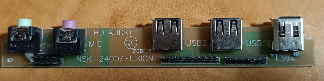
142.9 KB JPG
Anyone ever designed their own PCB?
Trying to replace the front IO Panel that supports a USB 3.0
Anyone know the name for Female 19 pin header?
Want to place it on the board so I can just use off the shelf USB 3.0 19 pin header extension cable.
42 RepliesView Thread
 Showing all 42 replies.
>>
>>
>>
File: file.png (798.9 KB)

798.9 KB PNG
>>2962516
Because it looks cool, and I'm reusing older motherboard.
Intel 8th gen.
It's going to sit under the TV as an emulator box and TV watching. The case supports IR remote and there's also VFD display! I want to see it in action
>>

>>
>>

>>
File: uFug mates.png (10.6 KB)

10.6 KB PNG
OP, what are you using to calculate the diff & single ended impedance of the USB data lines?
>>
>>2962509
There's nothing special about the PCB. You could just mount all the shit to a piece of protoboard that's cut to shape. Get protoboard with the correct pitch so you don't have to drill out holes to fit the jacks and pin headers.
>>
File: chip.png (349.8 KB)

349.8 KB PNG
>>2962574
They don't want you to know this but you can actually ignore line impedance and reflecting waves. The Smith chart is a tool made by big antenna to sell more antennae. Who is Smith anyway? Nobody knows. Electricity isn't a wave; I'd know, I'm a surfer. You actually don't need to know math to make a circuit. Just dabble 'till it works. That's what everyone does anyway. Math is for nerds. Don't be a nerd
>>
>>2962586
The PCB connects to the motherboard with shielded USB cables in the original PC. A couple of strips of copper foil tape for the ground plane is enough and if you use equal lengths of magnet wire flat against the protoboard it won't be an issue for OP's use case.
>>
File: file.png (121.8 KB)

121.8 KB PNG
>>2962551
Thanks anon, you just made me go down the rabbit hole.
Apparently my traces will need to be on 4 layer board.
2 layer board needs wider traces.
Used this calculator and PCBway formulas.
https://www.digikey.ca/en/resources/conversion-calculators/conversion- calculator-pcb-trace-impedance
https://www.pcbway.com/multi-layer-laminated-structure.html
>>
>>
File: 71ddhraQpBL.jpg (213.7 KB)

213.7 KB JPG
>>2962509
Fuck no. Fuck that. Absolutely the fuck not is it a beginner PCB design project. USB 3.0 is enough bandwidth to be a bitch about trace routing signal integrity shit.
Your best bet is ripping out the USB 2.0 components and bolting/gluing/bolting+gluing a premade molded cable to the PCB in their place, something like this.
It's what most off the shelf cases do for USB 3.0 front panel as well.
>>
File: file.png (125.8 KB)

125.8 KB PNG
>>2962731
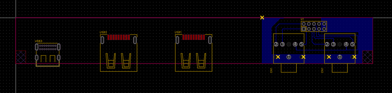
But anon, the whole signal integrity made me go down the rabbit hole of learning.
I think what I have should be good for 4 layer PCB
2 ground layers in the middle
I just now need to check it over and do all calculations. Hopefully i wired it up correctly.
>>
>>
>>
>>
>>
Dude just install kicad and figure it out
It has built in footprints for most connectors by name so you can drop one down and get a part number to go order.
It does differential signal trace length matching as well which you will need.
You could knock out a board in like 3 hours
You do not need 4 layer, skill issue and a half.
>>

>>

>>
>>
>>2962550
The reason he says that is that high speed digital signals turn everything into weird antennas and it's almost impossible for someone inexperienced to predict how it'll act, meaning it probably won't work. There are additional design rules for USB3 signalling and USB-C connectors like impedance matching, trace length matching, stub antennas, and so on. Have you looked at the implementation notes regarding ground plane (de)coupling? USB2 is comparatively much easier as even shitty designs will probably work.
>>
>>
File: file.png (3.2 MB)
3.2 MB PNG
>>2964480
Thanks.
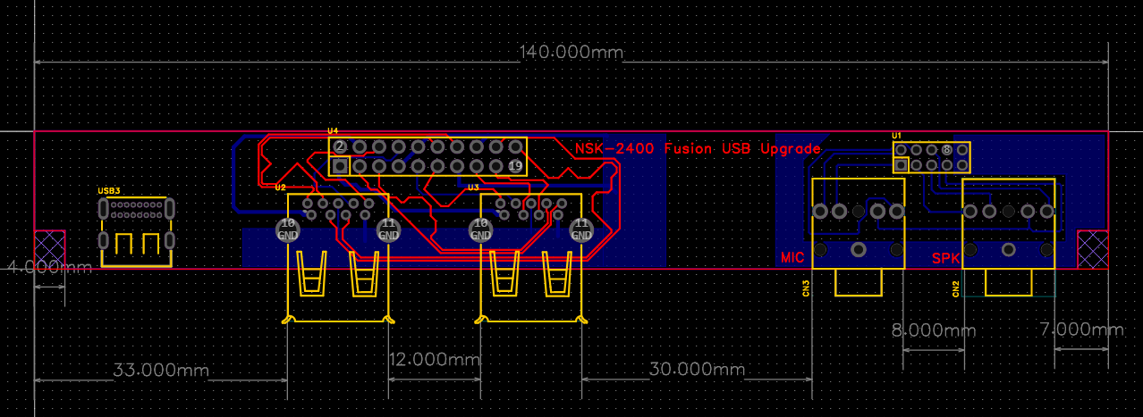
Surprisingly My traces are 0.5mm or more from each other and since it's 4 layer board, there's ground planes in between the traces on the other side.
Ordering the PCB today, with PCB assembly included. Will let you guys know if it works or I fucked up.
>>2964329
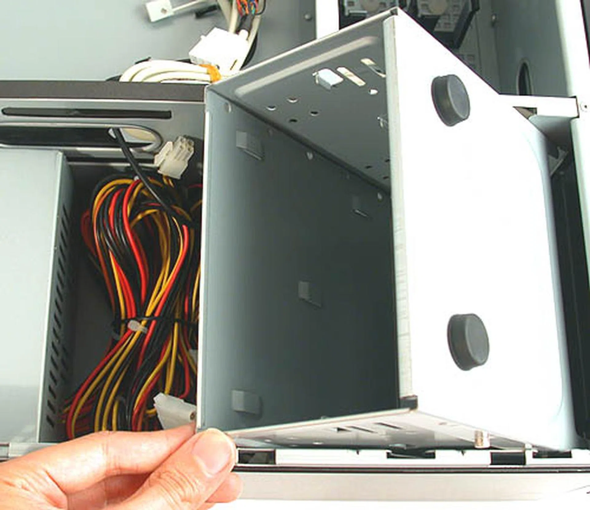
Yeah I got it for free, It's missing the cage for the DVD drive, so I'll need to think this one through, how to print it out on a 3d printer. (Pic related)
>>
>>2962530
love these cases lol. got a few on ebay for similar idea of upgrading them never got round to it. just use them to put hdmi out to digital signage instead of smart tv. look forward to see where this thread goes.
>>
File: Ordered.jpg (48.6 KB)

48.6 KB JPG
Ordered
>>
>>2964518
It's a very short adapter wire essentially so your chances are better than if you were designing a dense PCB but that spiderweb of traces with hard 90° bends all over the place and differential pairs not being routed in pairs half of the way and sitting right against other signal lines is not going to do you any favors. We don't make soft bends because they look pretty. We do it because once you get into the GHz range, the edges of traces become both emitters and reflectors and it starts to get properly weird.
>>
>>2964708
>than if you were designing a dense PCB but that spiderweb of traces with hard 90° bends all over the place and differential pairs not being routed in pairs half of the way and sitting right against other signal lines is not going to do you any favors.
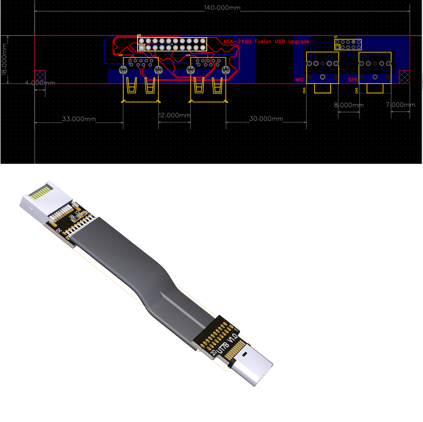
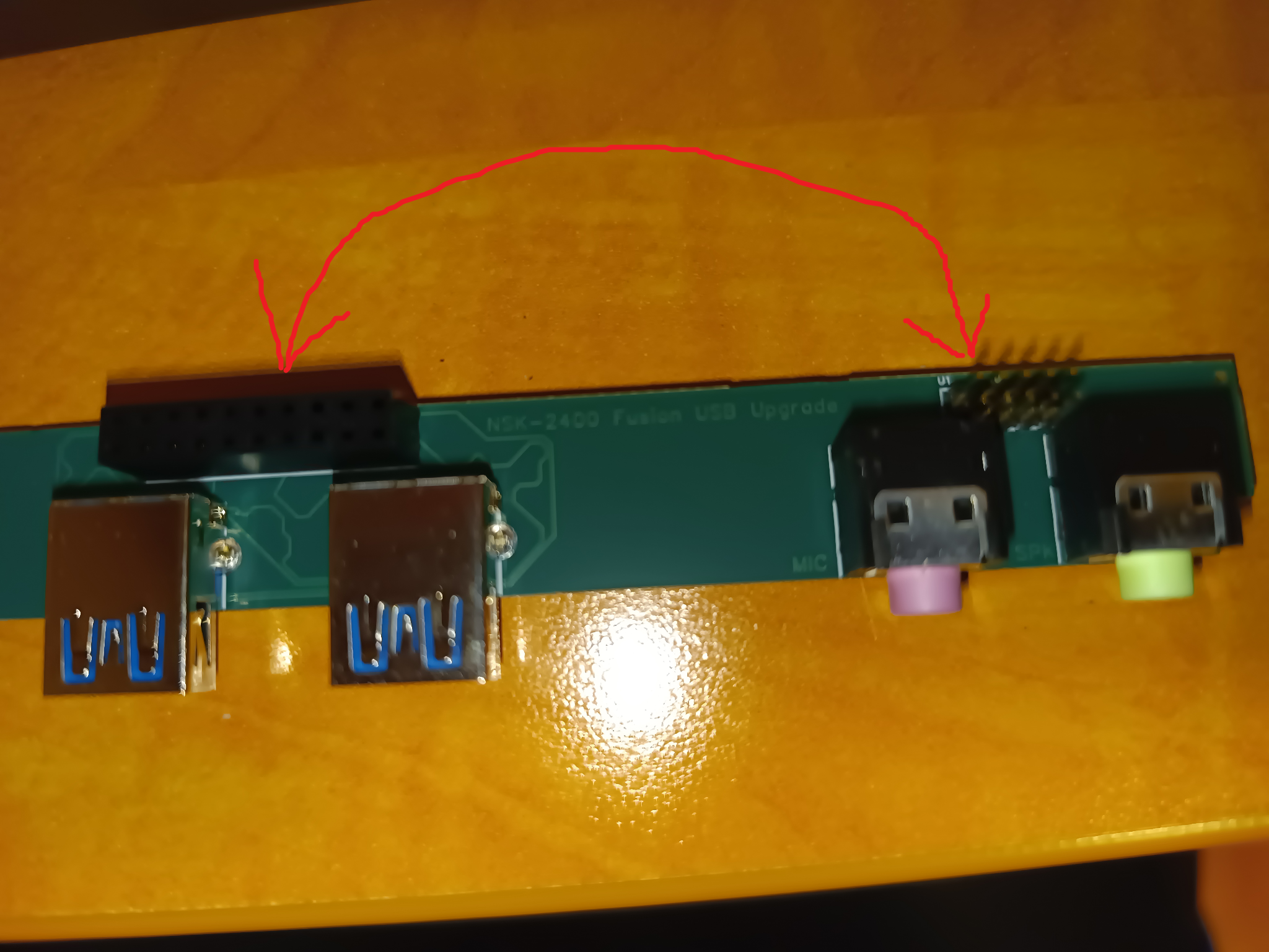
Interesting, yeah if I could I would have made the PCB larger for all of those traces. Having to fit it on 18mm pcb constrained a lot of my design choices.
If this is successful. I might try my hand on doing some USB routing board from scratch. Just to learn
>>
>>2964712
You don't need a bigger PCB. It's perfectly simple to route those traces sensibly on the one you have. You just need to have a general understanding of how signal lines interact with one another and to follow the design guidelines.
>>
File: Ordered2.jpg (124.3 KB)

124.3 KB JPG
PCB done
Assembly is next
>>
File: IMG_20251230_191423_750.jpg (499.1 KB)

499.1 KB JPG
>>2962509
They arrived!
>>
File: IMG_20251230_192352_776.jpg (780.7 KB)

780.7 KB JPG
>>2968177
FFUUUUUUUUUUCKKKKKKKK
THE CONNECTOR IS SLIGHTLY LARGER
FFFFFFFFFFFFFFFFFFFFFFFFFFFFFF
>>
>>
>>
>>
File: IMG_20260111_145849_581_1.jpg (1.5 MB)

1.5 MB JPG
>>2962509
IT'S WORKING!!!!!!!!!!!!!!!!!!
>>
File: Screenshot from 2026-01-11 15-01-00.png (131.7 KB)

131.7 KB PNG
>>2970352
>>
File: IMG_20260111_163202_256_1.jpg (1016.6 KB)

1016.6 KB JPG
>>2970353
>>
File: IMG_20260111_145913_921_1.jpg (563.8 KB)

563.8 KB JPG
>>2970354
Both ports are working!
Thanks everyone
>>
>>2962734
>Currently defense contractor building $2,000,000 36 layer high speed DDR5 and RF ipc cl3 boards designed to be thrown in the ground for 30 years and still have 100% fidelity.
I'm looking at this image of your layout and sensing you don't fully understand SI. The decoupling on those diffs are staggering, likely to have massive convergence issues. You'll be a lot better off running coupled serpentines. Also, place reference vias BEFORE routing. You should have every via you need placed before running traces.
>But I don't need vias
Clearly. We don't need to think about signal integrity. It's just modern made up jargon to sound important.